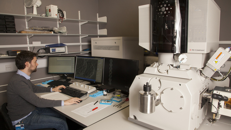
FEI Verios 460 scanning electron microscope
FEI Verios 460 scanning electron microscope (installed 2014)
- State-of-the-art, ultra-high resolution SEM for biological and material samples
- Accelerating voltage range of 1-30 keV, plus low voltage range of 350 – 1000 eV
- Probe current range of 0.78 pA – 100 nA
- Computer-driven, high precision stage with 360o continuous rotation and +60o to -10o stage tilt
- Everhart-Thornley (ETD) and Through-Lens detectors (TLD) for routine SE- and BSE-imaging in field-free mode (large field of view/depth of field) and immersion-mode (high resolution imaging)
- Concentric backscatter detector (CBS) for differential detection of BS electrons scattered at various angles from the beam axis; custom-mode allows selection of individual detector segments
- Mirror (MD) and In-column (ICD) detectors allowing detection of BS electrons for increasingly high Z-contrast imaging
- Beam deceleration mode (50 – 4000 V negative stage bias) for increasing resolution at low accelerating voltage settings; allows detection of near-surface electrons on flat samples
- Segmented STEM detector (STEM III) for TEM grid samples with custom settings for bright-field (BF), dark-field (DF) and high-angle annular dark field (HAADF) imaging
- UniColor mode (UC mode, monochromator, selectable below 5 keV/25 pA) to improve image quality at low keV/probe current settings
- Large range of image resolution and scan speed settings; custom settings for interlace scanning, multiple image integration and drift correction to improve image acquisition even of charging samples; definition of scan presets for easy and quick sample navigation and image acquisition
- Energy-dispersive X-ray detector (Ametek window-less silicon drift detector) for elemental analysis running with EDAX Genesis or TEAM software
- Cryo-SEM: Quorum cryo-transfer system PP3010T for loading, coating and imaging quick-slush frozen, hydrated specimens
- MAPS software for automated acquisition of high resolution images from large areas of SEM specimens or TEM blockfaces

